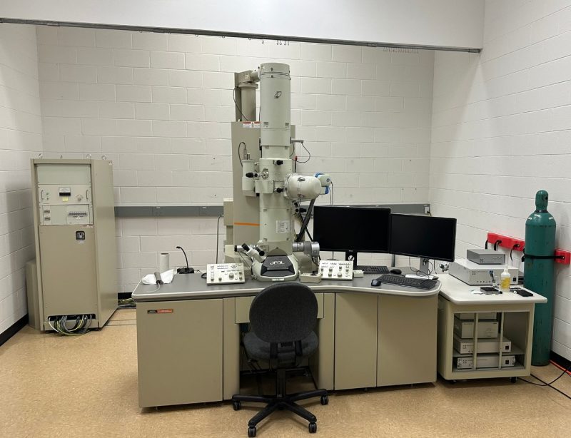
TEM: JEOL 2100

The JEOL JEM 2100 TEM is an analytical transmission electron microscope using a LaB6 electron source. This TEM was installed in 2016 for general day-to-day research and research training. TEM has been heavily used due to its STEM-EDS mapping (maximum resolution 5nm) and polymeric and biological samples imaging capabilities.
Contact: Hongyu Wang (hongyuw@vt.edu)
Location: ICTAS CRC room 1010A
- JEOL Genuine 60mm2 Silicon Drift Energy Dispersive X-ray (EDS) Detector
- JEOL Bright Field Detector for STEM imaging
- JEOL Genuine High Contrast (lower pole-piece) Aperture for enhancing image contrast in STEM-BF and TEM for polymeric and biological samples
- Variable accelerating voltages between 40 and 200kV
- Gatan Orius 833 Slow Scan CCD Camera (2048 × 2048 pixels) for recording images, electron diffraction patterns and large field of view imaging
- Gatan Ultrascan 1000XP CCD Camera (2048 × 2048 pixels, 14bit) for high resolution imaging (not recommended for SAED)
- Gatan Digital Micrograph ver. 3 (GMS-III)
- Shot Meister (SIF, Japan) Package for sequential (montage) imaging
- Spatial resolution (HRP, 200kV)
- TEM Point-to-Point. 0.23nm
- TEM Line 0.14nm
- STEM ~0.3nm (EDS 5nm)
Typical applications for this instrument are the imaging of soft and hard materials, diffraction analysis of crystalline materials, STEM-EDS chemical mapping, and general research.
This TEM is used for training, teaching and research/research education. Users can be trained to operate this instrument autonomously. Training for the first-step basic operation consists of 2 × 4-hour sessions (minimum). Additional training sessions will be required for advanced operation, such as EDS mapping, STEM imaging, and other modes.
- Maximum sample size: 3-mm diameter, 150 µm thick (including TEM specimen grid) and materials must be high vacuum compatible
- Biomaterials must be biosafety level 0 (BSL-0) or BSL-1 already prepared on a TEM grid. Toxic or potentially infectious biomaterials are not allowed.
- TEM images are a 2D projection of 3D specimens. This means that the images, diffraction information, or spectra information obtained by TEM is averaged through the thickness of the specimen, i.e., there is no depth sensitivity in a single TEM data. To minimize this projection effect, observation area needs to be thin and mechanically and structurally stable under the high energy electron beam.


