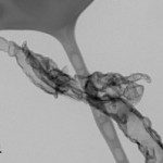
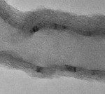
Philips EM 420
Contact: Hongyu Wang (hongyuw@vt.edu)
Location: ICTAS CRC room 1017
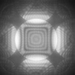
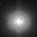
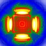
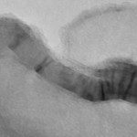
The Philips EM420 is a conventional TEM using a LaB6 electron source; it mainly focuses on BF/DF imaging and electron diffraction pattern recording. The microscope is capable of low acceleration voltage operation (from 40 up to 120kV), thus it is ideal for polymer, bio, and other electron beam sensitive materials. This TEM is also ideal for routine TEM investigations, sample surveysm and diffraction/imaging experiments requiring large tilt angles.
- Variable acceleration voltage from 40 to 120 kV (20kV is possible with ultra-thin sample);
- High sample tilt capability ±45°;
- Philips Single tilt multi-specimen holder;
- Philips Double tilt holder;
- SIA-8C slow scan CCD camera (2048 × 2048 pixels, 14bit) for recording images and electron diffraction patterns;
- Spatial resolution (120kV)
- TEM Point-to-Point 0.34nm
- TEM Line 0.1nm 0.20nm
This TEM is used for training, teaching and research/research education. Users can be trained to operate this instrument autonomously. Training for the basic operation consists of 2 × 4-hour sessions (minimum).
- Maximum sample size: 3-mm diameter, 150 µm thick (including TEM specimen grid)
- Biomaterials must be biosafety level 0 (BSL-0) or BSL-1 already prepared on a TEM grid. Toxic or potentially infectious biomaterials are not allowed.
- TEM images are a 2D projection of 3D specimens. This means that the images, diffraction information, or spectra information obtained by TEM is averaged through the thickness of the specimen, i.e., there is no depth sensitivity in a single TEM data. To minimize this projection effect, the observation area needs to be thin and mechanically and structurally stable under the high energy electron beam.
Sample Images
