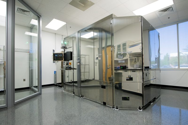
JEOL JBX-8100FS

The JEOL JBX-8100FS is an Electron Beam Lithography (EBL) tool.
EBL is a direct-write process that enables patterning on the nanometer scale. Like optical or laser lithography, EBL employs a photoresist-based technique but achieves features one hundred times smaller. This tool is optimized for both high throughput, with high maximum currents and dual current writing modes, and high resolution, utilizing a first in the U.S. 200kV electron beam.
Location: NCFL Room 1004
The JEOL JBX-8100FS is hosted at the NCFL but managed by the Department of Electrical and Computer Engineering.
To access/schedule this tool, contact Eric Carlson (ecarlson@vt.edu), Electron Beam Lithography Manager, Department of Electrical and Computer Engineering.
Additional Features
- 12 cassette automatic sample loader
- Temperature controlled enclosure maintains stage temperature drift <0.005 °C/hr.
- Internal optical microscope for sample/alignment mark locating
Specifications
- Accelerating Voltages: 100kV or 200kV
- Scan Speed: Up to 125 MHz
- Field Size: 50 µm x 50 µm (high resolution mode), 500 µm x 500 µm (high throughput mode)
- Stage Movement: 190 mm x 170 mm with 0.6 nm resolution
- Minimum Line Width: 8 nm
- Minimum Step Size: 0.5 nm
- Overlay Accuracy: ±6 nm (actual, high throughput mode)
- Field Stitching: ±16 nm (actual, high throughput mode)
- Sample Size: Up to 150 mm
Additional Facilities
- Beamer 7.1.0 pattern fracturing software with proximity effect correction (PEC)
- Photoresist spinning and development
- Optical microscopes and SEM available for exposure evaluation
Sample Image


