LEO (Zeiss) 1550
1550")
LEO (Zeiss) 1550: FEG-SEM equipped with EDS and EBSD
The LEO (Zeiss) 1550 is a high-spatial resolution SEM using a Schottky field emission (FEG) electron source, capable of resolution in 1-5 nm size range using an in-lens SED. It is used for high-resolution imaging of surfaces, qualitative assessment of the distribution of elements (by EDS), submicron structure analysis, and determination of crystal orientation and crystalline texture (by EBSD).
Contact: Stephen McCartney (stmccart@vt.edu)
Location: ICTAS CRC room 1016
TECHNICAL SPECIFICATIONS
- Accelerating voltage: 1kV to 30kV
- Detectors: 1 x In-lens secondary electron (SED), 1 x Everhart-Thornley secondary electron (SED), 1 x Robinson-type back-scatter electron (BSED)
- Energy Dispersive X-ray Spectroscopy (EDS): Oxford INCA E2H with INCAx-act 51-1385-005 Silicon Drift detector (SDD), Energy Resolution Mn K – 133eV, detection B - U, 0.1 - 1 at%
- HKL Nordlys II Electron Back Scatter Diffraction (EBSD) system, including a Forward Scatter Electron (FSE) detector
- Spatial resolution
- High-vacuum
- 1.0nm at 20kV
- 2.5nm at 1kV
- High-vacuum
NOTE: The effectiveness of low accelerating voltage operation depends heavily on the nature of a sample.
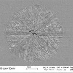
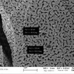
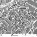
Sample Images